Optical Thin Film Metrology
Characterisation Installation 4
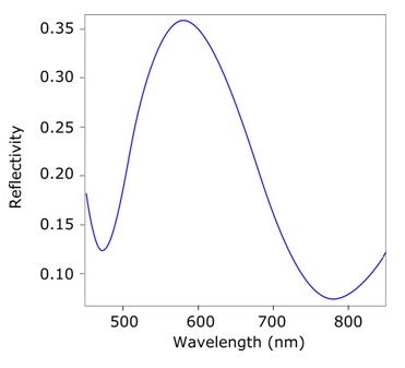
The principle of the thickness measurement is based on the interference patterns in the reflectivity spectrum of the layered sample. The measurement is performed without contact to the sample surface. Fast algorithms enable the performing pf the optical measurement and the calculation of the thickness with a high repetition rate and high reproducibility. In a typical configuration, the light reflected from the sample is collected by pick-up optics connected to the camera adapter of a microscope. An optical fiber guides the light to the spectrometer and the spectrum is detected by a high performance photo diode array. The measured spectrum from a layered sample shows typical interference effects which depend on the thickness and the optical properties of the materials. Therefore the film thickness can be determined if the optical properties and the sequence of films are known. Typical thicknesses between 50 nm and 20 μm can be measured with an accuracy of 1 nm. Examples of areas of applications include semiconductor technology (SiO2, Si3N4, resists etc), optical components, films on glass for liquid crystal displays, transparent coating on metals and other substrates etc.


