STM
Scanning Tunneling Microscopy
Characterisation Installation 4
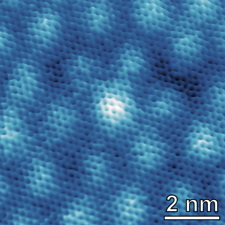
Scanning tunneling microscopy (STM) allows imaging conductive surfaces at the atomic scale. It is possible to characterize the distribution of surface terraces and steps, as well as to determine the atomic arrangement of (ordered) surface (over)structures.
In STM, an atomically sharp tip is scanned on a surface at a few-angstrom distance, while a bias voltage is applied between these two electrodes, so that a current flows due to the quantum tunneling effect. The intensity of the tunneling current depends exponentially on the tip-surface distance and can therefore be used to reconstruct a morphologic image.
STM is a local technique: while high-resolution can be achieved on small (nanometer sized) areas, information on large-scale (micron sized or more) is lost, and measurements have to be repeated systematically on several regions of the sample to get statistically relevant information.
Due to stability performances, STM experiments are typically time-consuming. The technique is applicable both in air and in vacuum. Ultra-high-vacuum (UHV) is required for the characterization of delicate, atomically clean systems.
The STM signal is not purely topographic, but brings also information on the local density of electronic states. Scanning tunneling spectroscopy (STS) is an extension of STM that provides information about the density of electrons in a sample as a function of their energy. Inelastic tunneling spectroscopy (IETS) is a challenging extension for the investigation of vibrational states at liquid helium temperature. The STM tip can also be used to manipulate single atoms and molecules.
By acquiring sequences of consecutive images, STM can also be used to investigate at the atomic scale dynamical processes occurring on the surface of conductive samples, with a typical acquisition time of few tens of seconds per image. To further extend the range of accessible details in this kind of measurements, NFFA-Europe makes for the first time available to external users the access to a FastSTM option for high-speed imaging with a VT-STM microscope at CNR-IOM. Thanks to this option, it is now possible to image with atomic resolution dynamical processes as chemical reactions, diffusion and growth, with a frame rate up to 100 images per second on regions few-nanometer wide.
Surface Science Lab @ Laboratory for Micro- and Nanotechnology
Temperature UHV STM/AFM @ DESY NanoLab
LT-STM
VT-STM
FastSTM

