Microluminescence
Characterisation Installation 5
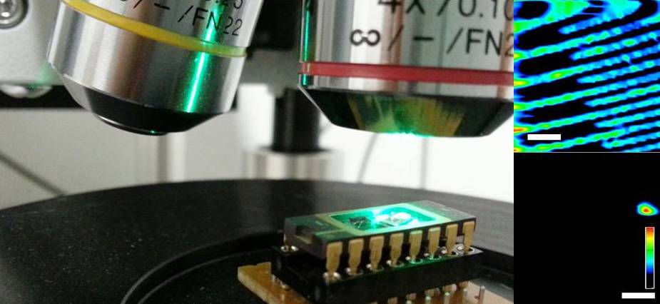
Semiconductors and fluorescent molecules are characterized by an energy gap between the highest occupied electronic state (HOMO in molecules and valence band in semiconductors) and the lowest unoccupied electronic state (LUMO and conduction band, respectively). When an electron is excited from the first to the second, after few nanoseconds relaxes to the equilibrium emitting a photon. This process takes the name of fluorescence in molecules and luminescence in semiconductors. The wavelength of the photon reflects the value of the energy gap, and in some specific samples also the energy of electronic defects in the gap, the electronic density state, the composition, the nanoscale structure, and so on. In case of semiconductors, often using a cryostage to operate at low temperatures increases the efficiency of the luminescence processes and improves the energetic resolution so that quantum effects can be investigated (for instance in quantum wells or quantum dots).
Electrons can be excited by shining photons with a wavelength shorter that that produced during the recombination. Usually to this purpose lasers are the best choice for their high intensity, but diodes or other sources are also employed (photoluminescence). Electrons can be directly injected in lowest unoccupied electron states, by electronic currents (electroluminescence), as in light emitting diodes (LED), or by exposing the sample to an electron beam (cathodeluminescence).
Using of a microscope to illuminate and/or to collect the light emitted from the sample allows to identify with sub-micron precision the region from where the light is emitted, and to acquire luminescence maps. This latter application is of particular interest for those structures, such as quantum wires and quantum dots, in which the luminescence spectrum of individual structures show properties that are averaged out by extensive measurements.