FIB
Focused Ion Beam

Lithography & Patterning Installation 1
add to your wishlist in your wishlist (remove)

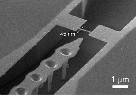
The common FIB Workstation is a high resolution FE-SEM combined with a FIB Ga+ column plus a multi channel gas injection system: Pt, C, W, Co, Au and SiOx are some of the usual precursors for ion or electron induced deposition (FIBID/FEBID); and Fluorine, Iodine or H2O are used for enhanced etching. It can be equipped with different detectors: Everhart-Thornley SE, In-lens SE detector, Backscattered Detector, EDX or STEM among others. Such systems are usually equipped with several nanomanipulators which allow both manipulation and electrical contacting in-situ, and an electron beam-blanker and nanolithography capabilities are also an option.

The main application areas are Nanofabrication and prototyping with nanometric resolution, FIB site specific cross sectioning and SEM inspection on a wide variety of samples (electronics, ceramics, metallurgy, biology…), TEM lamellae preparation, circuit editing and electrical and mechanical inspection in vacuum conditions, nanolithography both with ions or electrons... Actually, due to its high performance and accessories different applications are arising continuously.


WARNING: Access available only to CNR-IOM, but not for TEM sample preparation  

i
@
          provided at NFFA-Europe laboratories by:
Italy
CNR-IOM
Italy

LEO-ZEISS Cross-Beam 1540 XB system

High resolution imaging, nano-etching and –deposition, with Ga Ion beam

Ion gun: Ga+

Ion beam  voltage: 30 keV

Ion beam  current: 1pA – 500nA

SE and In-Lens detector available

Max. sample size 4"

EDAX EBS detector for chemical micro analisys

Fully integrated Raith Pattern generator for direct Ion Beam Lithography

CSIC
Spain

FIB - Zeiss 1560XB Cross Beam (N7)  

Fabrication of nanostructures by Ion-beam milling and e-beam/ion-beam deposition

Ga+ ion emitter, 1pA up to 40nA, and Schottky type electrons emitter, currents up to 10nA

For deposition, P, C and TEOS available, and XeF2 and H2O for enhanced etching

SEM variable from 0.1-30kV and FIB energy at 5 or 30kV

Up to 10nm resolution depending on the material and aspect ratio

Deposition resolution below 40nm

Mechanical Stage

Resolution below 1μm

Pieces from 2x2mm up to 6” wafers

HV, 10-6 mbar

SEM/FIB  inspection

Micromanipulators and feedthroughs for Lamela preparation or electrical contacts

CEA-LETI
France

Plasma FIB V-Ion FEI


Sample preparation for X-ray tomography, large or deep cross section (100µm or above), back side deprocess of silicon

Inductively coupled plasma (ICP) source from Xenon ions

Accelerating voltage from 2kV to 30kV

Maximum beam current at 30kV: 2µA

Secondary electron and secondary ion imaging

Maximum field of view 1mm2

Spatial resolution of 20nm

Motorized stage XYZ, rotation and tilt from -9 to 60deg

All types of sample, maximum size of 200mm with limited stage movement

Secondary vacuum (10-7Pa)

In-situ micromanipulator

In-situ and localized material deposition : Pt, SiOx

CEA-LETI
France

Strata 400 FEI

Sample preparation of TEM lamella, Electron tomography needle, Atom Probe needle, Cross section followed by SEM imaging

Liquid metal ion source from Gallium

Accelerating voltage from 0,5kV to 30kV

Secondary electron and secondary ion imaging

Images could be generated from the ion and the SEM column

Maximum field of view 1mm2

SEM resolution: 2nm

FIB resolution: 5nm

Motorized stage XYZ, rotation and tilt from -9 to 60 deg

All types of sample,  maximum XY size: 6.5cm, maximum height: 5mm              

Secondary vacuum (10-7Pa)

In-situ micromanipulator

In-situ and localized material deposition : Pt, SiOx, C, W