t-SPL
Thermal Scanning Probe Lithography
Lithography & Patterning Installation 1
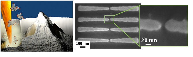
Thermal scanning probe lithography is a mask-less, serial and direct-write lithography technique, where a cantilever with a heatable ultra-sharp silicon tip (which is only a few nanometers in diameter) is brought into contact with a special resist that is spin-coated on a substrate. The horizontal and vertical motion of the substrate/tip can be controlled precisely by means of piezo stages and fast cantilever deflections, allowing sub-20 nm lateral and sub-2 nm vertical resolution. The electrostatic attraction between the cantilever and the workpiece bends the cantilever and brings the tip into contact with the resist.
At temperatures of up to 1000 °C the resist (polyphthalaldehyde, PPA) evaporates very efficiently and quickly (in less than 2 µs) without residues or contamination, leaving a tiny hole in the resist with the same geometry as the tip. No measurable mechanical force is acting between the tip and the resist during the patterning process. This step is repeated at speeds of up to several mm/s in order to create complex 3D surfaces.
An important aspect of the technology is the in-situ metrology during the writing process: With the tip in its cold state, the topography of each written line is read back by a second micro-heater which reads the distance to the surface by means of heat conduction through the air. The measured sub-nm deviations from the target are then used as feedback for the running patterning process (a technique called “Closed Loop Lithography”). Thus, accurate control with unmatched precision of the patterning depth is achieved.
The technique is compatible with standard clean room processes for pattern transfer, such as RIE, lift-off, electroplating, etc.