Atomic-to-microscale evaluation of large-area two-dimensional metal dichalcogenides for microelectronics

Understanding the process-structure-property relationship from bulk to atomic scale is crucial for developing and optimizing the fabrication process for novel electronic materials especially in the field two-dimensional transition metal dichalcogenide layers, which exhibit unique properties down to one-atomic thickness. As the large-scale production method for such 2D materials are at its infancy, many of their properties and effect of the process parameters are largely unknown. Most of the current characterization method that is being utilized for evaluating the material property is limited to certain length scale and specific properties of the material. More than one characterization techniques are needed for the proper interpretation of the data and efficient development of the material synthesis method.
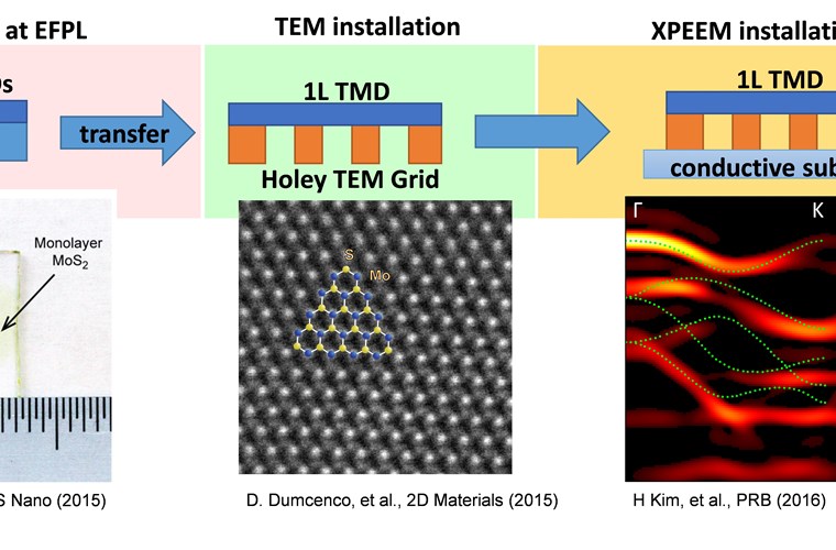
Toward this end, under the NFFA-Europe scheme, we have performed the same-area characterization of atomic-structure properties such as point-defect densities and impurities, and micro-scale electronic properties such as electronic band-structure and work function on pristine and electron irradiated freestanding MoS2 produced by chemical vapor deposition (CVD). This in-depth, multi-lateral characterization was carried out through two NFFA-user access facilities, transmission electron microscopy (TEM) installation and photoelectron emission microscopy (PEEM) installation, at CEA-Grenoble in France.
The sample was prepare by transferring CVD MoS2 layers grown on c-sapphire onto customized, conductive, silicon nitride TEM grids with arrays of 20 µm-diameter holes. High-resolution STEM imaging was first performed to observe the intrinsic atomic structure followed by in-situ electron irradiation to control the defect densities within the suspended membrane of atomically thin MoS2. The same sample was next analyzed by PEEM for the influence of the defect density on the electronic band structure and work function of the pristine and electron irradiated areas of freestanding MoS2 layers.
Further measurement is underway to take a full-advantage of the same-area, correlative characterizations using spatially resolved photoluminescence/Raman spectroscopy, X-ray photoemission spectroscopy for wider range of length scale and properties to fully understand the role of the defects in determining the quality of the large-scale application of two-dimensional materials.

