Block co-polymer lithography is made available at NFFA Europe for large area nano-patterning
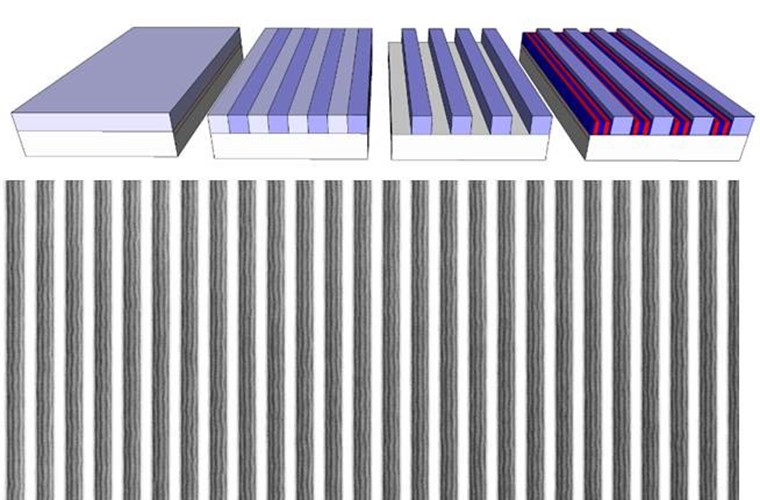
Directed self-assembly (DSA) of block copolymers is a method of creating polymer patterns over large areas with a resolution of less than 10 nm. The beauty of the method is its inherent simplicity: block copolymers in solution are deposited by spin coating onto a surface; after a short thermal annealing under ambient conditions, the polymer molecules self-assemble to form patterns whose dimensions are defined by the size of the molecules. If the receiving surface features ad-hoc manufactured patterns (so-called guiding patterns), the self-assembly follows the directions dictated by the guiding patterns. In this way, dense arrays of ordered polymeric lines and cylinders are obtained.
Even in its simplest form without guiding patterns, block copolymer lithography has applicability in many areas, such as the creation of nanostructured surfaces of controlled wettability or the fabrication of nano-porous membranes. By incorporating guiding patterns, more complex structures can be made, such as dense arrays of nanomechanical and nanoelectronic devices.
"Having now the block copolymer lithography available within NFFA on the CSIC site in Barcelona will allow to address many interesting applications for which a nanoscale pattern covering large areas is needed ", says Perez-Murano.
DSA of block copolymers can compete with state of the art industrial solutions for high volume manufacturing in terms of resolution and throughput, as EUV optical lithography and DUV immersion optical lithography. But, until now, defect generation during the self-assembly has prevented its incorporation into semiconductor foundries.
"Having now the block copolymer lithography available within NFFA on the CSIC site in Barcelona will allow to address many interesting applications for which a nanoscale pattern covering large areas is needed "
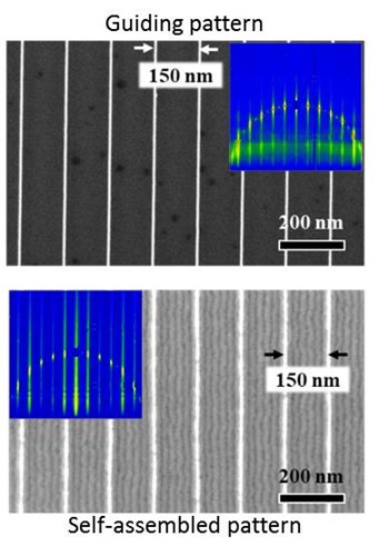
Collaborative work among multiple NFFA laboratories has revealed a mechanism for defect formation. The research is based on the creation of very precise guiding patterns. By analyzing the density of defects after self-assembly, the correlation between variations in the dimensions of the guiding patterns and the appearance of defects has been established.
“The analysis of the results has made it possible to expand the existing free energy self-assembly models by adding the energy contribution of the defects. As a result, the process window can be predicted precisely, ”says Steven Gottlieb, a former doctoral student at the CSIC who participated in this research
In the course of the investigation, two nanolithography methods have been developed to create high-precision guiding patterns:
- High-accuracy SiO2 patterns with trenches ranging from 68 nm to 117 nm width were fabricated by exposing a hydrogen silsesquioxane (HSQ) resist using EUV-interference lithography. The accurate control of the space between two guiding pattern ridges and their extremely low line edge roughness has allowed to analyze the response of the block copolymer molecules under confinement. It has been investigated how the accuracy of the resulting patterns dimensions allow achieving low defectivity line/space patterns of a PS-b-PMMA (polystyrene-block-poly methyl methacrylate) block copolymer of 11 nm half.
- SiO2 lines less than 10 nm wide were fabricated by electron beam exposure of HSQ. The extreme resolution obtained has made it possible to study the influence on the appearance of defects when the critical dimension of the guiding pattern (linewidth) is of the same order as the size of the block copolymer molecules.
(*) CSIC-Institute of Microelectronics of Barcelona; PSI-Laboratory for Micro- and Nanotechnology; DESY-Deutsches Elektronen-Synchrotron
Block copolymer lithography based on High resolution EBL guiding patterns
Credit: Steven Gottlieb and Francesc Perez-Murano
Soft Matter, 2018, 19, 14, 6799-6808. DOI:10.1039/C8SM01045E
Nano-confinement of block copolymers in high accuracy topographical guiding patterns: modelling the emergence of defectivity due to incommensurability
S. Gottlieb et al.
Mol. Syst. Des. Eng., 2019, 4, 175-185. DOI:10.1039/C8ME00046H
Self-assembly morphology of block copolymers in sub-10 nm topographical guiding patterns
S. Gottlieb et al.
Facilities:
Cleanroom at PRUAB-Institute of Microelectronics of Barcelona, CSIC in Spain. Swiss light source (SLS) synchrotron and Clean room of the Paul Scherrer Institute in Switerland, and the Nanolab Institute and PETRA III at DESY in Germany.
Techniques:
Block copolymer lithography, Electron Beam Liuthography. Atomic Force Lithography and Anisotropic Oxygen Plasma Etching at PRUAB-CSIC; XIL-II beamline with an open access tool of EUV interference lithography at PSI; Electron Beam Lithography (Vistec EBPG 5000+ tool at 100 kV) at PSI; GISAXS measurements performed P03 Micro- and Nanofocus X-ray Scattering Beamline at PETRA III at DESY
Francesc Perez-Murano
Francesc Perez-Murano is research professor at IMB-CNM, CSIC. He has been involved in nanofabrication research and development since 1989.
Steven Gottlieb
This work is part of the PhD thesis of Steven Gottlieb. The thesis has received the best thesis year award by the Electronics Engineering Department at the Universitat Autònoma de Barcelona
Francesc Perez-Murano Francesc.Perez@csic.es
IMB-CNM, CSIC, Carrer dels Til·lers s/n. Campus de la Universitat Autònoma de Barcelona, E-08193 Cerdanyola del Vallès, Spain.

