Atom Probe Tomography
Characterisation Installation 4
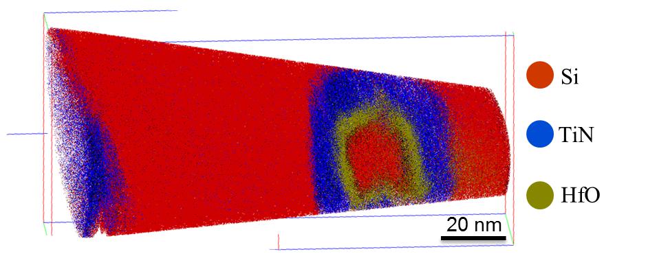
Atom probe tomography uses a voltage and/or laser pulse to field evaporate atoms from the end of a specimen in the form of a sharp tip. The tip must have an end radius of less than 50 nm and may be prepared by electro-polishing (metallic samples) or by FIB (other sample types and when site specificity is required). By measuring the time-of-flight and the position of the evaporated atoms on a position sensitive detector a 3-D reconstruction of the position and chemical nature of detected atoms is possible. The technique has sub-nm resolution (around 0.1-0.3nm resolution in depth and 0.3-0.5nm laterally) and detection efficiencies as good as 80%. The mass resolution of a typical instrument is between 1000 to 2000 m/dm. The use of laser pulsing allows metals, semiconductors and insulators to be analysed. However, samples that contain a mix of insulators, semiconductors and metals can be challenging and sample fracture may occur at weak interfaces.
CAMECA / FLEXTAP laser assisted tomographic atom probe
An IR/vis/UV fs laser is used to controlled and assist the field evaporate atoms from the end of a sharp tip held at high voltage
Here are the different wavelengths that can be used to assist the field evaporation:
IR = 1030 nm
Green = 515 nm
UV = 343 nm
The detector is an advanced delay line detector (ADLD) that is able to detect the 2-D position of ions hitting the detector as well as the flight time that is used to calculate the mass-to-charge ratio of each detected ion
The detection efficiency is approximately 62%
The field of view is adjustable from 8° to 30°
The analysed volume is typically 100 x 100 x 200 nm3
The spatial resolution is anisotropic: 0.3 nm along the depth axis (O,z) and 0.5 nm along (x,y) plane
The mass resolution at FWHM is < 3000 m/Δm
The area of interest must be placed at the end of the sharp FIB (Focused Ion Beam) prepared tip
The accuracy of placing the feature of interest is sample dependent, typically of the order of 50 nm
The sample must be prepared by FIB (so the initial wafer or sample must be cut to a size suitable for FIB, typically a few mm or cm in size)
The APT analyzed volume at the end of the FIB prepared tip is in the range of 100 x 100 x 200 nm3
Samples should be vacuum compatible
Oxides metals and semiconductors can be analyzed
Heterogeneous samples may lead to reconstruction artefacts that result in distorted 3-D volumes, this depends strongly on the relative evaporation fields of the materials in question
APT analysis is controlled using acquisition software which is supplied by CAMECA
Parameters which can be controlled are the electric voltage, energy laser, temperature and evaporation flux
Analysis chamber is UHV (1E-11 mbar)
A combination of a standing high voltage (1-15 kV) and a femtosecond laser pulse is used to evaporate atoms from the tip of the sample
The sample is cooled during analysis to reduce thermal vibrations (12 to 70 K) but the temperature at the tip can momentarily reach 300K during laser pulsing

