Cathodoluminescence
Characterisation Installation 4
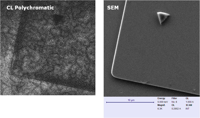
The cathodoluminescence tool is a SEM with a FEG source (3-10 keV) allowing spatial resolution as low as 3 nm. Samples are mounted on a 1 inch sample holder attached on a piezoelectric nano-positioning cryostage allowing low temperature measurements (~10K). An intra-column optical collection system coupled with a dispersive spectrometer and two array detectors permits the spectral analysis of luminescence emission from 200 nm to 1.6 µm. This system offers a way to extract spatially resolved electronic and/or optical properties of luminescent material and devices.
Cathodoluminescence
Helium to room temperature luminescence characterization of solid samples
Analysis of material properties (charge carrier recombination, electronic transition) and detection of defects or impurities
Electron gun with a beam current varying from 100pA to 20nA, focused on the sample thanks to a SEM microscope

