AFML
Atomic Force Microscopy Lithography
Lithography & Patterning Installation 1
SPM in ambient conditions
Atomic Force Microscopy (AFM) in contact or dynamic modes for topographic characterisation can work in parallel with other surface properties: conductivity (C-AFM), electrostatic force (EFM), surface potential (KPFM), magnetostatic force (MFM), capacitance (SCM), spreading resistance (SSRM), piezoelectric response (PFM).
Oxidation Scanning Probe Lithography (o-SPL)
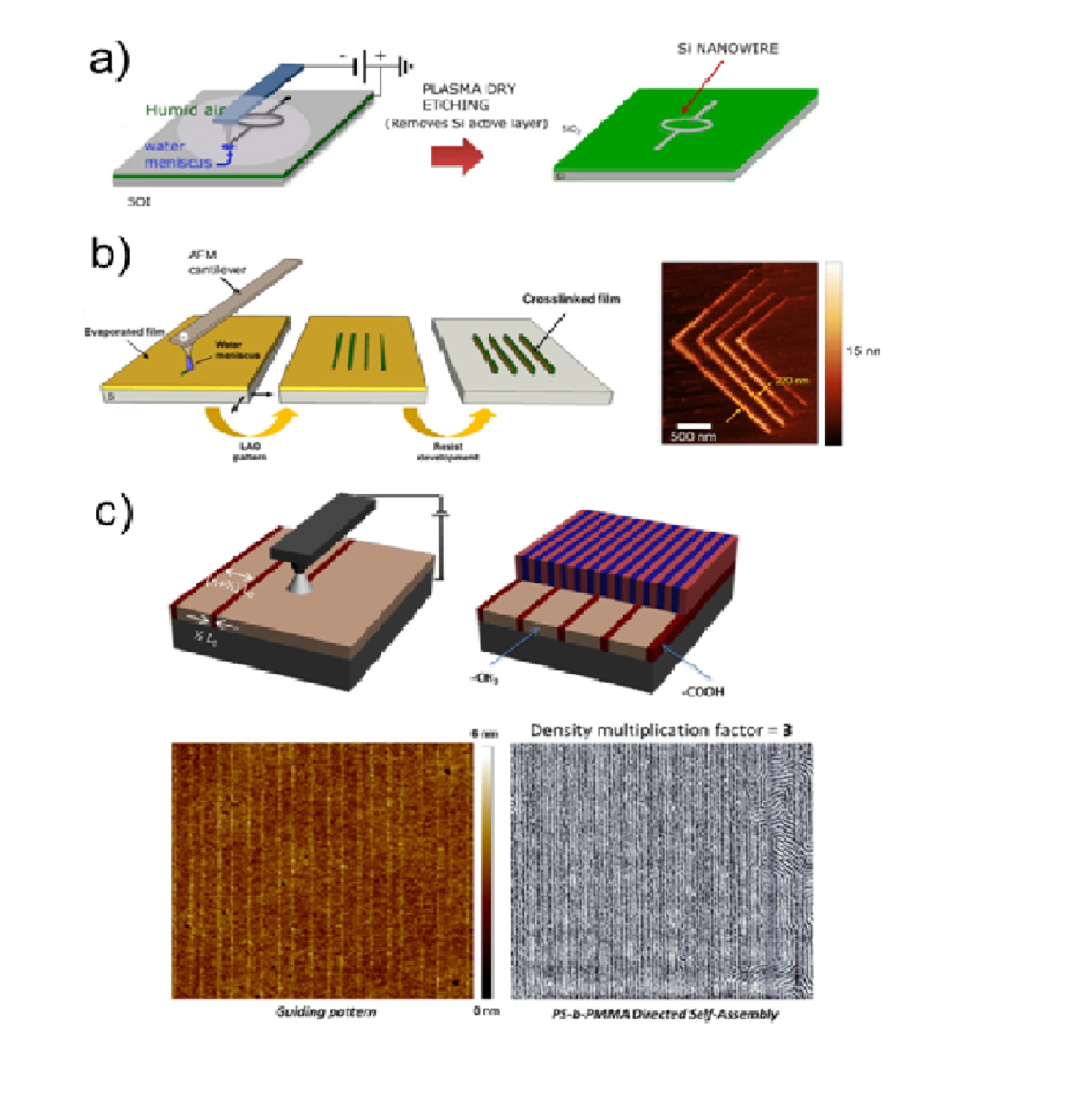
O-SPL nanolithography possesses the versatility to pattern a wide range of materials, including metals, semiconductors, polymers and biological molecules in different media. O-SPL allows the confined oxidation of the substrate underneath the tip by the ionization of the water neck present in ambient condition. By means of O-SPL integrated with other fabrication steps, it is possible to produce a wide variety of functional electronic and mechanical nanostructures. as for example: dielectric barriers, masks for selective etching and templates. Devices include ultra-small Si nanowires, by combining O-SPL with plasma dry etching.
It is possible to use O-SPL to locally crosslink a resist in a negative tone fashion. This is achieved by designing a specific molecular resist able to crosslink by oxidation and then developing the film.
O-SPL in non-contact mode can also create chemical patterns on a surface with sub-10 nm resolution. The surface can be locally oxidised to change its interaction force with other entities. For example, the modified surface can selectively change the attraction towards polymers chains, to single lines of molecules or as guiding patterns for directed self-assembly of block co-polymers.

AFM Veeco IV + Dimension 3100 controller (N8)

