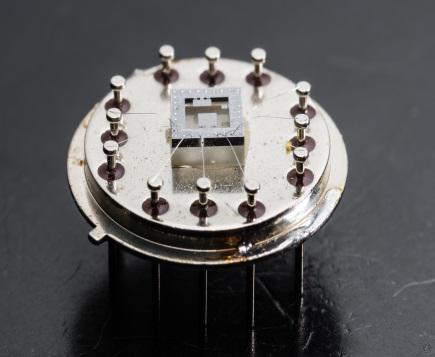
Chip packaging
Lithography & Patterning Installation 1
Chip packaging is the last process in the fabrication flow of an micro-nanodevice. It consists in the chip insertion in a substrate aimed to:
a) Make the chip functions easily accessible (electrical connection with the real world),
b) facilitate its handling for its assembly onto an electronic system
c) preserve the chip from external agents and increase its durability.
Hence the importance of the packaging in the final behavior of a device or circuit is very high, since the packaging can heavily affect the yield and performance of the device in several aspects as its thermal dissipation capability, its electrostatic discharge resistance or its number of outside connections.
Several important steps of the packaging process can be distinguished: the substrate (silicon or others) dicing with manual or automatic saws, the die attach by manual or automatic pick and place or flip-chip techniques, the electrical connection (wedge, ball and ribbon bonding with different wire materials and diameters) and the final encapsulation and package quality test (die shear and pull test).
K&S 4xxx Series
LoadPoint 3AV14 / K&S 980-10

