EBL
Electron Beam Lithography

Lithography & Patterning Installation 1
add to your wishlist in your wishlist (remove)

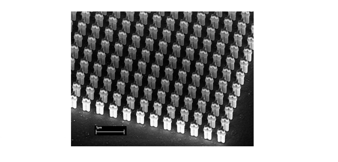
A typical electron beam lithography tool is a vector-scan direct write tool with a Gaussian shaped beam. The electrons are accelerated to typically 50 keV or 100 keV and the beam scanning is controlled by a combination of usually two deflection systems. The beam is directed to a position in the main deflection field (with a maximum size of a few 100 µm²), where a pattern is written by stepping around the electron beam.  For larger patterns, the pattern is divided in main field blocks, which are completely exposed one-by-one after moving the substrate to the right position. A laser interferometer can often measure the actual stage position, and this signal is fed back to the deflection system with sub-nm resolutions.


The electron beam stepping frequencies can be as high as 50 MHz, which provides relatively high speed direct nanopatterning. The electron beam spot size can be focused to sub-10 nm in diameter. Owing to the wide range of available beam currents (typically 200 pA – 200 nA), high-throughput as well as high-resolution exposures are possible. With high accelerating voltages, thick layers of e-beam resists can be exposed with small forward electron scattering. Electron-beam lithography systems typically have small overlay precisions and can handle full wafers, mask blanks, and custom shaped samples. Typical features can include automatic laser focusing for height measurement, and manual or automatic detection of alignment markers for multiple lithography level processes. Users can implement or supply their designs in most standard formats.


WARNING: Access to CNRS temporarily not available

i
@
          provided at NFFA-Europe laboratories by:
Italy
France
Spain
Sweden
Switzerland
LU
Sweden

EBL - Voyager  (44)

High speed EBL exposure of electron beam sensitive resists 

Schottky type filament, currents up to 10nA with fast electrostatic deflection coils

Fixed at 50kV

20nm resist lines

Laser interferometer stage for stitch accuracy of about 25nm, 400um writefield size

Pieces from 2x2mm up to 6” wafers

Hi-vac, E-7 mbar

Laser height sensor for automatic large area exposure

LU
Sweden

EBL - Raith (101)

EBL exposure of electron beam sensitive resists 

Schottky type filament, currents up to 400 pA with slow magnetic deflection coils

Variable from 3-20kV

15nm resist lines

Laser interferometer stage for stitch accuracy of about 25nm, 100um writefield size

Pieces from 2x2mm up to 6” wafers

Hi-vac, E-6 mbar

PSI
Switzerland

EBL - Vistec/Raith EBPG 5000+ ES system @ Laboratory for Micro- and Nanotechnology

Electron Beam Lithography

Electron gun

100keV accelerating energy, 200pA-200nA beam currents

Interferometric stage

<5nm spot size

512x512 μm2 max main field, 50 MHz max stepping frequency, overlay precision <20nm for 100x100 μm2 field

Any chip size, wafers up to 150mm and 5" x 5" mask blanks, automatic 10-position air-lock

UHV

LayoutBEAMER software for pattern generation/proximity effect correction, L-Edit CAD tool for pattern design/import

Spin-coating, metal evaporation, etc.

CNR-IOM
Italy

EBL - LEO-ZEISS Cross-Beam 1540 XB system

High resolution SEM with focused ion beam column (FIB) and gas inlet system (GIS)

Electron Beam and Ga ion beam

Voltage range of the electron beam is from 0.7-30kV

Probe current (10pA - 5nA) with high stability (0.2%/h)

Ultimate resolution of 1 nanometer

Max writing field 1mm

Stitching precision 1micron

Blanker frequency: 1MHz

The maximum host sample is 4" wafer

The write filed size of the single EBL exposure is 1mm2 

ELPHY Quantum Plus is lithography hardware attachment: Hierarchical fully integrated GDSII layout editor/viewer, exposure parameter adjustment and calculation, 300 kHz maximum writing speed, digital image acquisition

CSIC
Spain

EBL - FE-SEM LEO 1530 + Elphy Plus (N6)

SEM inspection for CMOS and non-CMOS samples and EBL exposure of electron beam sensitive resists

Schottky type filament, currents up to 2nA

0.1- 30 kV

100μm write-field for high resolution up to 1mm

No stitching capabilities

~ 1nm in SEM and below 30 nm resist lines

Mechanical Stage, resolution below 1μm

Pieces from 2x2mm up to 4” wafers

HV, 10-6 mbar

SEM inspection

Spinners and hot-plates for resist preparation

CSIC
Spain

EBL - Raith 150 TWO (N2)

EBL exposure of electron beam sensitive resists 

Schottky type filament, currents up to 10nA

Variable: 0.1-30kV

100μm or 200μm write-field for high resolution up to 1mm

10nm resist lines (depending on resist and thickness)

Laser interferometer stage for stitch accuracy below 20nm in 100μm or 200 write-field sizes

Pieces from 2x2mm up to 6” wafers

HV, 10-6 mbar

Inspections

Large scan maps due to stitching resolution

Spinners and hot-plates for resist preparation