Ion implantation
Lithography & Patterning Installation 1
The implanted ionic species are obtained from gas or solid precursors and directed towards a substrate that is scanned under the beam. The implant dose (amount of dopants) and energy (related to the depth they will penetrate) are the main parameters of the implantation process. The time it takes to reach a given dose (and, in this way, the range of practical doses) will depend on the current capabilities of the implanter (medium, high current). After the implant the samples need to go through a thermal process to heal the crystalline damage (amorphization) and to allow the dopant elements to take substitutional places in the crystalline network (electrical activation). Ion implantation allows dopant concentrations above the solid solubility limit. Amorphous substrates can be implanted, too, in search of a change of properties. Selective implant can be achieved by means of a masking material with a thickness enough to block 99.99% of the impinging ions at given implant conditions.
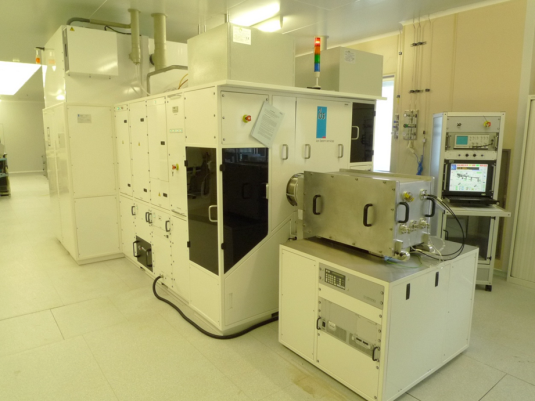
IBS IMC 210 RD

