PL
PhotoLuminescence
Characterisation Installation 5
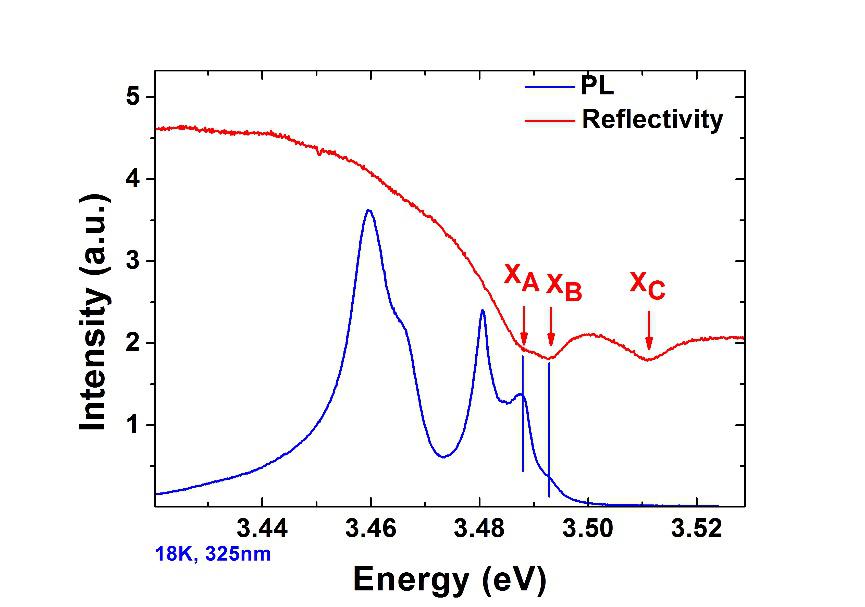
PL is a non-contact, non-destructive method of probing the electronic structure of materials. Incident photons are directed onto a sample where they are absorbed (photo-excitation) and the sample will then release photons. Quantum mechanically PL can be described as an excitation to a higher energy state and then a return to a lower energy state accompanied by the emission of a photon. Available energy states and allowed transitions between states are determined by the rules of quantum mechanics. The period between absorption and emission is typically extremely short, in the order of 10 nanoseconds.
PL is often used in the context of semiconductor devices where the energy of the incident photons is above the bandgap energy. PL spectra are useful to determine the bandgap energy, the composition of heterostructures, the impurity levels, the crystal quality, and to investigate recombination mechanisms.
Several variations of photoluminescence exist: in the photoluminescence excitation (PLE) the spontaneous emission from the sample is detected at fixed photon energy and recorded as a function of the pump frequency; time-resolved photoluminescence (TRPL) is where you excite luminescence in a sample with a light pulse and then look at the decay in photoluminescence with respect to time.
WARNING: Access to CNRS temporarily not available, but the technique is available at the other sites
Micro-photoluminescence
Helium to room temperature luminescence characterization of solid samples
Analysis of material properties (charge carrier recombination, electronic transition) and the detection of defects or impurities
Multiple laser sources with optical power at the sample between 1 and 10 mW are focused on the sample using a confocal microscope

