SEM
Scanning Electron Microscopy

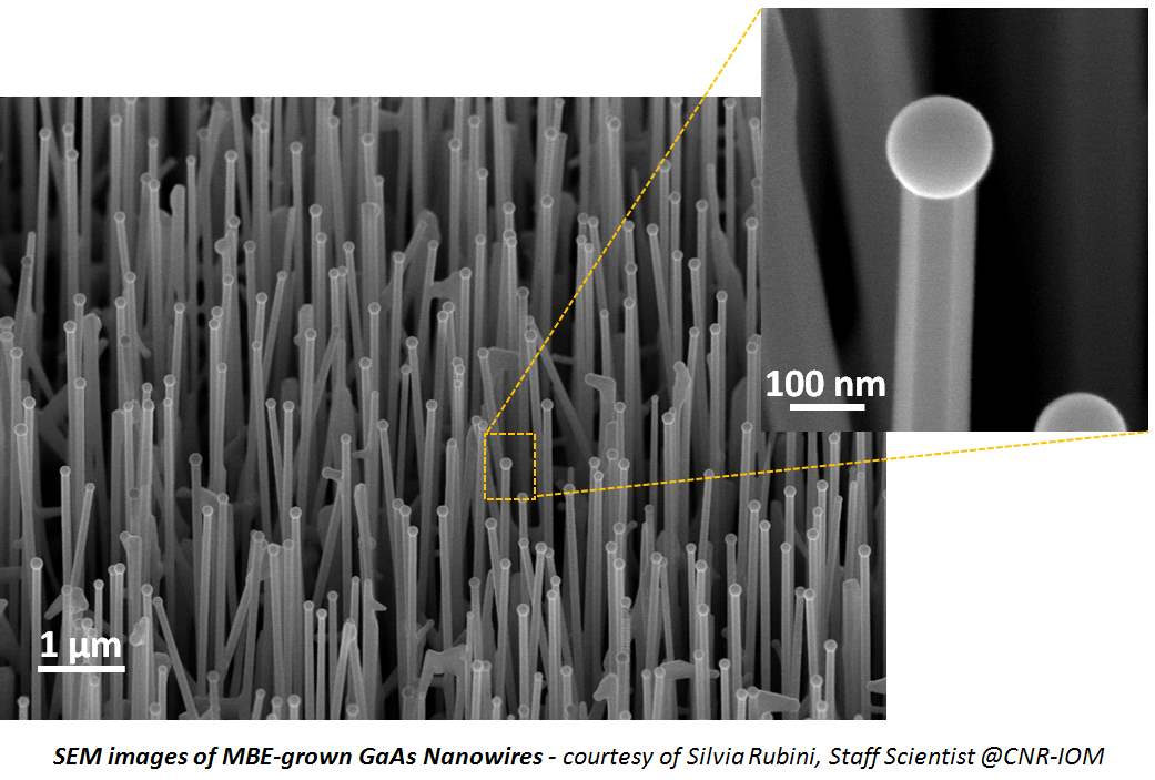
Characterisation Installation 4
add to your wishlist in your wishlist (remove)

In a SEM, a beam is scanned over the sample surface in a raster pattern while a signal from secondary electrons (SE) or Back-scattered electrons (BSE) is recorded by specific electron detectors. The electron beam, which typically has an energy ranging from a few hundred eV up to 40 keV, is focused to a spot of about 0.4 nm to 5 nm in diameter. Latest generation SEMs indeed can achieve a resolution of 0.4 nm at 30 kV and 0.9 nm at 1 kV.

Beyond the ability to image a comparatively large area of the specimen, SEM can be equipped with a variety of analytical techniques for measuring the composition, crystallographic phase distribution and local texture of the specimen. Chemical composition analysis can be performed by Energy Dispersive X-ray Spectroscopy (EDS) which relies on the generation of an X-ray spectrum from the entire scan area of the SEM. An EDS detector mounted in the SEM chamber collects and separates the characteristic X-rays of different elements into an energy spectrum and EDS system software is used to analyse the energy spectrum in order to determine the abundance of specific elements. EDS can be used to find the chemical composition of materials down to a spot size of a few microns and to create element composition maps over a much broader raster area.

An SEM complemented with a (FIB) focused ion beam permits in addition an in-depth analysis by creating a cross-section cut that is subsequently analysed using the electron beam and the SEM/EDS detectors (slice&view). In a similar way, a 3D tomography can be generated by an iterative ion beam milling and electron beam imaging. Furthermore, the ion beam permits to cut a thin lamella out of a sample surface that could be taken out by a micro-manipulator and analysed with the electron beam in transmission using a so called STEM (scanning transmission electron microscope) detector.


WARNING: Access to CNRS temporarily not available, but the technique is available at the other sites

@
          provided at NFFA-Europe laboratories by:
France
Italy
France
Spain
Germany
Greece
Spain
Sweden
Switzerland
Spain
ICN2
Spain

SEM – FEI Quanta 650 FEG ESEM

High resolution surface imaging, low vacuum imaging, environmental SEM capabilities and chemical composition analysis

Schottky field emission gun

Beam voltage: 200V to 30kV

Beam current: 1.6pA to 200nA

Secondary electrons (SE)

Backscattered electrons (BSE)

Transmitted electrons (STEM)

Energy Dispersive X-ray Spectroscopy (EDX)

0.8 nm @ 30kV (STEM)

1.0 nm @ 30kV (SE)

3.0 nm @ 1kV (SE)

Up to 8” diameter flat samples

High vacuum: 10-4Pa

Low vacuum: 10Pa – 130Pa

Environmental mode: 10Pa – 4000Pa

Environmental mode: sample cooling (down to -25ºC), heating (up to 1000ºC) and wet samples imaging

ICN2
Spain

SEM – FEI Magellan 400L XHRSEM

Extreme high resolution surface imaging

Schottky field emission gun with monochromator (UniColore electron source)

Beam voltage: 50V to 30kV

Beam current: 1.6pA to 26nA

Secondary electrons (SE)

Backscattered electrons (BSE)

Transmitted electrons (STEM)

0.8 nm @ 30kV (STEM)

0.8 nm @ 15kV (SE)

1.5 nm @ 200V (SE)

Up to 4” diameter flat samples

High vacuum: 10-4Pa

High resolution imaging of insulating samples (no coating needed)

In-situ plasma cleaner

LU
Sweden

SEM - LEO 1560

SEM inspection

Standard Schottky type filament

Beam voltage: 0.5-30kV

ET and through the lens type detectors

1.3nm at 20kV

150mm travel of stage

From stubs up to 6” wafers

High Vacuum only: E-6 mbar

LU
Sweden

Hitachi SU8010  

SEM inspection

Cold field emission type filament

Beam voltage: 0.1-30kV (good imaging at low kV)

ET and through the lens type detectors

STEM detector (BF and DF)

1.1nm at 20kV

60mm travel of stage

From stubs up to 4” wafers

High Vacuum only: E-6 mbar

LU
Sweden

JEOL JSM-6700F SEM

Imaging and analysis at the sub-micron-level via SEM and EDXS

Field emission gun

Up to 30kV accelerating voltage

Back scattered electron detector

Secondary electron detector

EDXS detection on 50mm SSD from Oxford Instruments

Image resolution is sub-10nm

Spectral resolution: 130eV approx. on EDXS

SEM sample can be moved plus/minus 10mm in X and Y

Working distances variable from around 3 to 15mm

Standard SEM samples

Standard vacuum in the microscope column

Sputter coating for insulating specimens

UAB
Spain

SEM – Zeiss Merlin

SEM analysis

Field Emission Gun

Beam voltage: from 0.5 kV to 30 kV

Beam current: from 20 pA to 40 nA

Secondary Electrons Detectors: ET and In-lens

Backscattered detectors: ASB (Standard detector) and ESB (Energy Selective Backscattered)

X-Ray detector EDS Oxford LINCA X-Max

Low voltage imaging

0.8nm at 15kV, 1.4nm at 1kV

5 axis motorized eucentric specimen stage

Max size: 130x130x50mm  

High vacuum

Pd/Au coating, embedding, polishing

Ultramicrotomy

PSI
Switzerland

Zeiss Supra 55 VP @ Laboratory for Micro- and Nanotechnology

SEM

Schottky field emission electron gun, Gemini column

0.1-30keV

In-lens SE detector

Chamber Everhart-Thornley detector

Retractable backscattered electron detecor (high keV)

Variable pressure (low vacuum detector)

1 nm (15keV), 1.7 nm (1keV)

Fully motorized stage,with tilt and rotation, several sample holders (flat, tilted)

6" wafer loadable and partially covered, 4" fully observable, various chip sizes

Chamber camera

High vacuum

Cr sputter coater for charge compensation

CEA-LETI
France

Hitachi H5500 High resolution SEM

SEM

Cold Field Emission Gun

High tension from 0.5 to 30 kV

Secondary and backscattered electron detectors

STEM detector

0.4 nm at 30 kV

1.6 nm at 1 keV

Inlens pole piece

Small samples (5mm)

DESY
Germany

SEM @ DESY NanoLab

Imaging of surfaces in reflection mode, in scanning mode and scanning transmission microscopy (STEM), elemental analysis by EDX (point and line analysis, mappings)

High resolution field emission instrument Nova Nano SEM 450 (FEI)

Acceleration Voltage: 200 V - 30 kV

Deceleration mode

Current up to 200 nA

EDX: 127 eV @ MnKα

SE Everhart-Thornley detector (ETD)

Low vacuum BE detector

High resolution through-lens detector tunable for SE and BE mode

High resolution STEM detector for analysis of membranes and thin films in transmission

X-Max 150 EDS silicon drift detector for elemental analysis, energy resolution 127 eV @ MnKα (Oxford)

IR-CCD camera to track the sample position

Lateral resolution:

1.0 nm at 15 kV

1.4 nm at 1 kV

0.8 nm at 30 kV (STEM)

Possible translation of sample stage in x/y: 110 x 110 mm

Navigation and pattering software

Sample tilt -15° to +74°

All materials

Sample sizes 100 mm x 100 mm x 50 mm (length x width x height)

Ambient temperature

Cross-section thickness measurement software

10-5 mbar typical operating pressure

Plasma cleaning

Gas injection system for electron beam induced deposition (EBID) with Pt precursor material to write Pt based markers on sample  surfaces, as e.g., markers for Nanopositioning to be developed within Joint research action 5 "Advanced Nano-object Transfer and Positioning"

CNR-IOM
Italy

SEM-EDX

Scanning electron microscopy with energy dispersive X-ray microanalysis

High brightness field-emission gun (FEG)

Beam voltage: 0.02- 30kV

Beam current: Configuration 1: 4pA -20nA/Configuration 2:12 pA – 100nA

High efficiency in-lens detector

Everhart-Thornley Secondary Electron Detector

Cap mounted AsB detector

CCD-camera with IR illumination

1.0 nm at 15kV

1.9 nm at 1kV

5-Axes Motorised Eucentric Specimen Stage: X = 130 mm, Y = 130 mm, Z = 50 mm, T = -3 - +70°, R = 360° (continuous)

6-Axes Eucentric Stage: X = 100 mm, Y = 100 mm, Z = 42 mm, Z’ = 13 mm, T = -4 to 70°, R = 360° (continuous)

STEM detector (scanning transmission electron microscopy)

SDD EDX system for chemical micro-analysis with 10 mm2 active area, energy resolution for Mn Kα: 129 eV or better, peak shift and resolution change <1 eV

CNR-IOM
Italy

FIB-SEM

Focused Ion Beam-Scanning Electron Microscopy

Ga focused ion beam (FIB)

High brightness field-emission gun (FEG)

Beam voltage: 30 KeV (FIB); 0.7-30kV

Current voltage: 1pA – 500nA (FIB); 10pA - 5nA with high stability (0.2%/h)

Everhart Thornley

In-lens secondary electron

Pattern generator for electron beam and Ga ion beam lithography

EDX system for chemical micro-analysis with 10 mm2 active area, energy resolution Mn Kα: 150 eV or better

CSIC
Spain

FE-SEM LEO 1530 + Elphy Plus (N6)

SEM inspection for CMOS and non-CMOS samples

Schottky type filament

0.1- 30 kV

Currents up to 2nA

100 μm writtefield for high resolution up to 1mm

No stitching capabilities

~ 1nm in SEM and below 30 nm resist lines

Mechanical Stage, resolution below 1μm

Pieces from 2x2 mm up to 4” wafers

High Vacuum: E-6 mbar

SEM inspection and EBL exposure of electron beam sensitive resists

Spinners and hot-plates for resist preparation

CSIC
Spain

QUANTA FEI 200 FEG-ESEM

Imaging, size, morphology and microstructure; high-profile nanostructural characterization; non-destructive analytical techniques (imaging and microanalysis); nanometer level inspection of materials, lithography and nanolithography

Field Emission Microscope, Zirconium Tungsten filament

Accelerating voltage: 200V – 30kV

Probe current: up to 100nA 

EDT - Detector Everhart Thornley: high-vacuum mode, EDX mode, RAITH mode

BSED - Solid State Backscatter Detector: high-vacuum mode, low-vacuum mode, EDX mode, RAITH mode

CCD - Infrared inspection camera: high-vacuum mode, low-vacuum mode, Environmental mode, RAITH mode 

LFD - Large Field detector: low-vacuum mode, EDX mode

GSED - Gaseous Detector: Environmental mode


High-vacuum: 1.2nm at 30kV (SE), 2.5nm at 30kV (BSE), 3.0nm at 1kV (SE)

Low-vacuum: 1.5nm at 30kV (SE), 2.5nm at 30kV (BSE), 3.0nm at 3kV (SE)

Environmental mode: 1.5nm at 30kV (SE)

EDX mode: energy resolution of 132 eV, chemical analysis with a high lateral resolution (point analyses and elemental mapping)

Degrees of freedom x, y, z, rotate 360º, Tilt (+85º, -10º)

Conducting materials (High-vacuum)

Uncoated non-conducting materials (Low-vacuum, Environmental mode)

Complex multi-component nanostructured materials (EDX)

Chamber pressure monitored by water vapour injection, 10 to 200 Pa (Low-vacuum)

Study samples in pressures up to 5 Torr

Chamber pressure monitored by water vapour injection (Environmental mode)


Specific holders (High-vacuum, Low-vacuum, Environmental mode)

Software EDAX GENESIS (EDX)

Software ELPHY Plus 5.0 (RAITH)